Orca Hana is an MCU module board based on the PIC18(L)F45K50 Because it was designed in a compact and durable module form, a single module can be reused across many different hobby projects and experimental applications. The PIC18(L)F45K50 is a small yet highly versatile MCU equipped with most of the features commonly needed for hobby electronics, including Full-Speed USB, PWM, USART, I2C, SPI, 10-bit ADC, and DAC. Even today, it remains a very capable MCU for small embedded systems, DIY electronics, and experimental projects. Orca Hana was designed using KiCad, and all design files and related resources will be openly shared.
Design Philosophy of Orca Hana
FCG (funcoolgarage.net) aims for the simplest possible design with the highest possible usability.
Hobbycentrism
All development directions at FCG (funcoolgarage.net) are focused on hobbyists. We call this philosophy hobbycentrism. Unlike commercial mass-production environments, hobbyists are free from many practical restrictions and can fully express their own ideas, creativity, and individuality. Orca Hana is FCG’s first open hardware project, and it was designed with hobbycentrism in mind from the very beginning.
Reusability
Because Orca Hana was designed as a detachable module, it can be connected to various motherboards and reused across many different applications. It can also be mounted on universal PCBs or breadboards, making it suitable for many kinds of prototypes and experiments. A single module can cover the entire development process, from circuit design and testing to protocol verification and even application development. This provides both convenience and cost reduction at the same time.
Reducing Build Cost
Orca Hana was designed as a compact 4-layer PCB while still maintaining practical usability. In the future, higher-performance processor modules will likely require much higher integration density and significantly more expensive multi-layer PCBs. However, the motherboards used to host those modules can still be built using relatively inexpensive 2-4 layer PCBs. Hence, modular development can minimize the size of expensive high-layer-count PCBs and help reduce overall build costs for hobbyists.
Hardware Overview
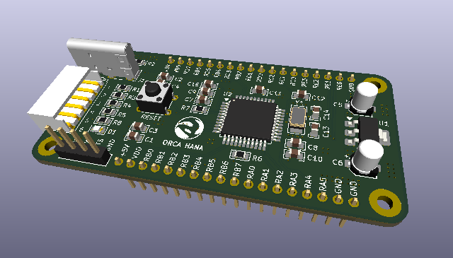
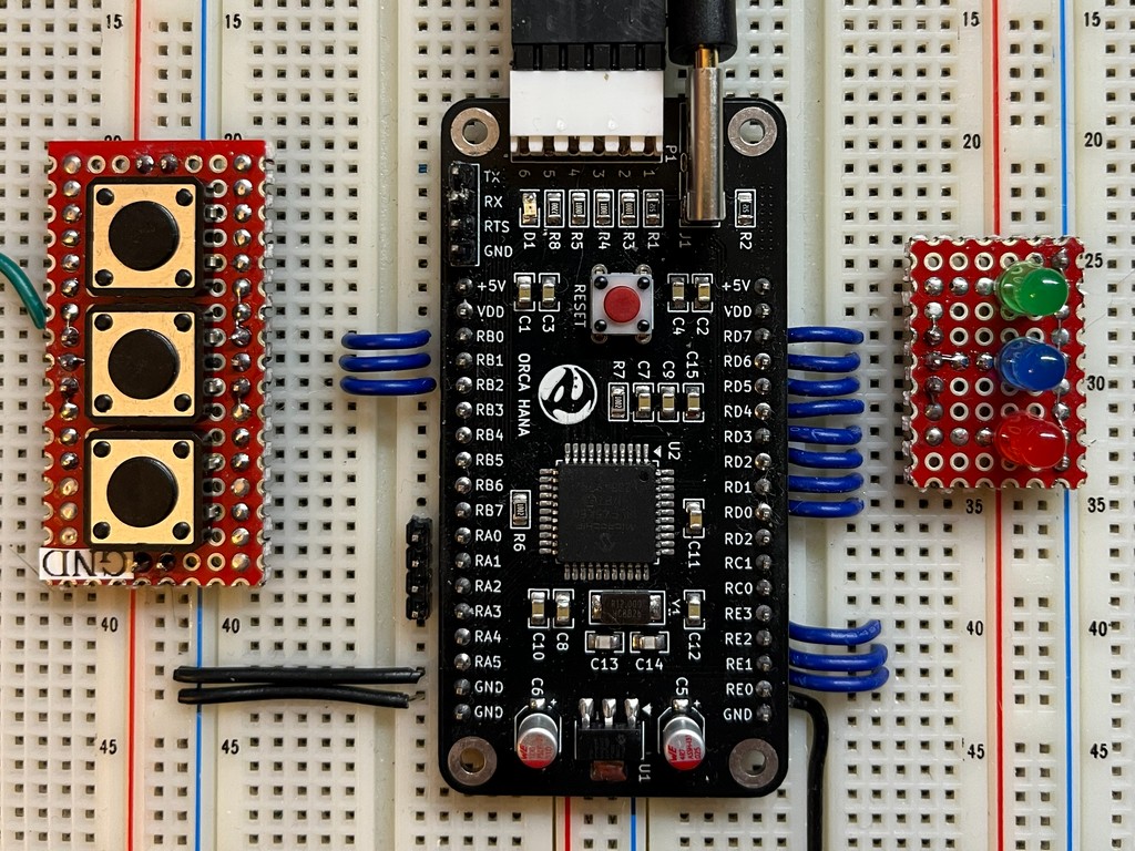
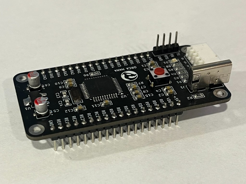
Orca Hana is a PIC18(L)F45K50 MCU module board with a size of 71.1 x 35.6mm. It provides a total of 30 I/O pinouts, all arranged with a standard 2.54mm pitch, making them fully compatible with universal PCBs and breadboards. Because of this, Orca Hana can be easily mounted on a universal PCB or breadboard for quick protocol testing and hardware experiments. Fig. 2 shows an Orca Hana module mounted on a breadboard while running a USB HID test.
Available Memory
Orca Hana provides enough memory for a wide range of applications, including USB stack-based systems and many other embedded projects. The PIC18(L)F45K50 used in Orca Hana includes the following memory resources:
- Program Memory: 32KB
- RAM: 2048 Bytes
- Data EEPROM: 256 Bytes
If additional memory is needed, external serial RAM/NVRAM or serial EEPROM devices can also be added to the application board, making it easy to expand the system memory as needed.
Operating Voltage of Orca Hana
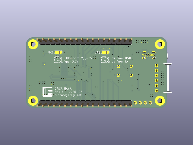
Orca Hana is an MCU module board designed to operate from a 4.5V ~ 5.5V power source, and it supports both the PIC18LF45K50 and PIC18F45K50 devices. The LF device operates within a voltage range of 1.8V ~ 3.6V and supports XLP (Extreme Low-Power) management features. The F device operates within a voltage range of 2.3V ~ 5.5V. Although it does not support XLP features, it is necessary when true 5V I/O operation is required. Orca Hana supports both chipsets, and jumper settings located on the back side of the board allow users to select the MCU operating voltage as well as the power source, either USB 5V or an externally supplied 5V source.
Clock Source of Orca Hana
The PIC18(L)F45K50 includes factory calibration and self-tuning features, allowing USB communication to operate reliably at Full-Speed (12Mb/s) even when using the internal oscillator. However, to support applications requiring a more accurate clock source and to improve the robustness of USB communication, a 12MHz external crystal was added to Orca Hana. When driving USB communication using the external 12MHz crystal, the register settings are configured as follows:
#pragma config PLLSEL   = PLL4X
#pragma config CFGPLLEN = ON
#pragma config FOSC     = HSH
// CPUDIV is not relavent to the USB clock settings. it only decide the cpu clock.
Pinouts and Reset
Orca Hana adopts a USB Type-C receptacle in order to follow modern USB trends. However, the PIC18(L)F45K50 only supports USB 2.0 Full-Speed operation, so when connecting Orca Hana to a PC with a traditional USB Type-A port, a USB-C to USB-A cable is required. Please note that the USB cable must support data communication and should not be a charge-only cable.
A dedicated UART pinout is also provided for debugging purposes. To connect Orca Hana to a PC through UART, a USB-to-TTL cable is required, and users should verify whether the cable supports 5V or 3.3V operation. USB-to-TTL products using the FTDI FT232RNL are recommended.
For convenience, Orca Hana also includes essential features such as a RESET button and Power LED, as well as ICSP (In-Circuit Serial Programming) and ICD (In-Circuit Debugging) interfaces for PIC programming and debugging.
Finally, buttons and LEDs on Orca Hana were intentionally minimized. Additional buttons and LEDs, such as bootloader-related controls or application-specific indicators, are expected to be implemented on the motherboard depending on the requirements of the application.

Example Applications
Built-in Peripheral Blocks
Orca Hana, powered by the PIC18(L)F45K50, can be considered a versatile low-power 8-bit MCU module board thanks to its wide variety of built-in peripheral blocks. In addition to its built-in Full-Speed USB block, it includes peripherals such as ADC, DAC, and PWM for sensor signal processing, motor control, and signal generation. The MCU also provides built-in blocks such as latches, comparators, and voltage detectors that are useful for signal sensing, conditioning, limiting, dimming, and charge-time measurement. Because of this, Orca Hana can be applied to a wide variety of applications without requiring many external components. The built-in peripheral blocks are listed below:
- Universal Serial Bus
- Up to 30 configurable GPIO
- SR Latch
- Enhanced Capture/Compare/PWM(ECCP)
- Master Synchronous Serial Port(MSSP)
- Two Analog Comparators with Input Multiplexing
- 10-Bit Analog-to-Digital(A/D) Converter module - Up to 25 input Channels
- Digital-to-Analog Converter(DAC) module
- High/Low-Voltage Detect module
- Charge Time Measurement Unit(CTMU)
- Enhanced USART module
More detailed information about each peripheral block can be found in the PIC18(L)F45K50 Microchip documentation.
The USB 2.0 transceiver built into the PIC18(L)F45K50 allows Orca Hana to communicate with PCs through various USB classes such as MSC, HID, and CDC. Using the built-in ADC, DAC, comparator, latch, and voltage detector blocks, users can build front-end interfaces for external sensors. The built-in PWM can also be used for motor control. Because of this, Orca Hana can be used to build many kinds of USB-connected applications involving sensor reading, motor control, signal generation, and experimental embedded systems.

In addition, the PIC18(L)F45K50 used in Orca Hana includes serial interface blocks such as I2C and SPI. Through these interfaces, various peripheral devices such as LCD modules, serial EEPROMs, serial SRAM, and RTC modules can easily be connected. Communication modules such as WiFi can also be added, allowing the application range of Orca Hana to be expanded even further.
Why PIC?
The Orca series at FCG refers to a family of 8-bit MCU boards based on PIC microcontrollers. Orca Hana is the very first board developed in the Orca series, and “Hana” means “one” in Korean. Considering both versatility and USB 2.0 support, the PIC18(L)F45K50 was selected as the first MCU for the Orca series module board.
PIC devices are RISC processors with a relatively small instruction set, which gives them a simple and efficient hardware structure. One of the major characteristics of PIC MCUs is that many of their peripheral blocks operate independently from the processor core. PIC devices also provide configurable I/O with a wide operating voltage range, stable temperature characteristics, and built-in ESD protection against static electricity. Because of these features, PIC MCUs have already been widely adopted in industrial equipment and automotive systems where durability, stability, and reliability are extremely important.
Some of the strengths of PIC MCUs can be summarized as follows:
- Durability, Stability, and Reliability
- Independent Peripheral Blocks with Rich Functionality
- Extreme Low Power
- In-Circuit Programming (ICSP) and Debugging (ICD)
The fact that PIC MCUs are already widely used in automotive and industrial equipment says a lot about their industrial-level durability and reliability. In other words, PIC MCUs are already well proven in terms of long-term stability and dependable operation.
PIC MCUs include independently operating embedded peripheral blocks such as USB SIE, Enhanced USART (RS-232, RS-485), MSSP (SPI, I2C), and USB support. Because many functions are handled directly by hardware peripherals, complex operations can often be implemented with relatively small and efficient firmware. These independent I/O blocks help reduce both firmware size and processor overhead.
Current consumption in standby mode is typically around 0.3~4uA, which is significantly lower than many general-purpose MCU families. In particular, LF devices such as the PIC18LF45K50 used in Orca Hana support nanoWatt eXtreme Low Power (nanoWatt XLP) technology. In sleep mode, current consumption can be as low as 20nA, and around 300nA while the Watchdog Timer is running. In addition, the CPU, SRAM, and peripheral modules can each be independently disabled, allowing power consumption to be optimized for low-power applications.
Because programming and debugging can be performed using only two signal lines (clock and data), circuit design becomes much simpler and fewer package pins are wasted. In addition, low-cost and easy-to-use tools such as PICKIT 3/4/5 allow convenient programming and debugging through MPLAB X IDE or MPLAB VSCode.
Development Environment
The development environments for PIC devices include MPLAB X IDE and MPLAB for VSCode. MPLAB X IDE is Microchip’s traditional desktop development environment based on NetBeans. On the other hand, the newer MPLAB for VSCode is provided as an extension for VSCode, allowing many of the features previously available in MPLAB X IDE, such as MCC and debugging tools, to be used directly inside VSCode.
In particular, the Clang/LLVM (Low-Level Virtual Machine) support provided by MPLAB is compatible with the XC compiler toolchain, allowing developers to take advantage of various LLVM-based features. In addition, AI-assisted extensions available in the VSCode ecosystem can also be used, making the overall development environment both convenient and modern.
MPLAB for VS Code Information Link
All Resources Will Be Openly Shared
All design resources provided by FCG will be openly shared under the Creative Commons Attribution (CC BY) license. This means the materials can be freely used and modified as long as proper attribution is provided.
- GitHub Repository
- Possibility of Finished Product Sales
- Questions and Answers
All development work at FCG is publicly available on GitHub. Users who are interested can access the repositories through the FCG resource pages and clone the repositories directly. The repositories include all files required for DIY development, including KiCad design files, PCB Gerbers, schematics, BOM files, and related project resources.
For users who find PCB manufacturing or component assembly difficult, inconvenient, or time-consuming, FCG may also provide assembled PCBs or fully completed products in the near future.
Questions can be discussed through the future Q&A board or through article comments. FCG will do its best to provide helpful answers whenever possible. However, FCG is not a commercial support service, and discussions are intended to be collaborative rather than authoritative. Since nobody knows everything, it would be great if people could explore and discuss solutions together.
Final Thoughts
Orca Hana was designed with versatility and reusability in mind. In order to make the board useful for both beginners who are just getting started with PIC devices and experienced hobby developers, the module form factor felt like the most practical approach.
Since Orca Hana is still based on an 8-bit MCU, the hardware structure itself is actually quite simple, almost simple enough to make people wonder whether a dedicated PCB is even necessary. However, following the philosophy of “simple is beautiful,” unnecessary complexity was intentionally minimized while maximizing usability and durability.
This design philosophy will continue into future 32-bit ARM module boards as well. DRAM and components requiring timing-sensitive high-speed I/O will be mounted directly on the module itself, while fine-pitch BGA packages may eventually require PCB stack-ups with as many as 12 layers. Because of this, the modular design approach is expected to become even more valuable for hobby developers in terms of both cost reduction and reusability.
Development Resource Links
Development resources for Orca Hana are publicly available on GitHub. Anyone is free to download and use the materials through the FCG resource links below as long as proper attribution is provided.
Post your comment